Unpacking the NVIDIA H100 Tensor Core GPU: A Deep Dive for CTOs
NVIDIA H100 Models: Specifications and Use Cases
If you have ever dealt with NVIDIA's top-end GPUs as part of your day-to-day work life, you'll have noticed there is more than one H100 (or perhaps you haven't!). The product naming scheme for these GPUs is super confusing, so I thought I'd consolidate some of my notes here to help others be aware of and hopefully understand a little better the confusing landscape that is NVIDIA's H100.
There are five (ish) commonly available SKUs of H100 that you are likely to see. I'll go through them in some detail below, but the basics of it are as follows: H100 SXM, H100 PCIe (with or without NVLink), H100 NVL, and GH100 (Grace Hopper).
Follow-up post to come on the H200 variants as we see them publicly announced and not subject to NDA.
1. NVIDIA H100 SXM5
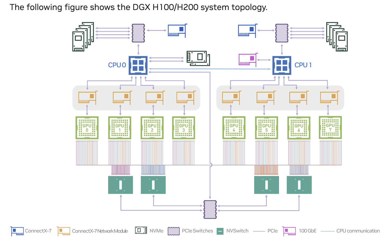
This is probably the most popular chip; it's what most of the big LLMs are being trained on. It's the ‘flagship’ GPU today from NVIDIA. This is an interesting GPU because it's not a ‘typical’ GPU in the sense that it's a PCIe card you can install into a slot in a server. It's shipped as a set of 8 GPUs all glued to a single baseboard that is then installed into a specifically designed server from an OEM (think Dell, HP, SuperMicro, ASUS, etc).
- Form Factor: SXM5
- Memory: 80 GB HBM3
- Memory Bandwidth: 3 TB/sec
- NVLink Speed: 900 GB/sec
- PCIe Gen5 Speed: 128 GB/sec
- TDP: Up to 700W
- Use Cases: Large-scale HPC simulations, AI foundational model training, drug discovery, and materials science.
Pros:
- Superior memory bandwidth and capacity.
- Higher TDP allows for more intensive computations.
- Enhanced scalability with NVLink and NVSwitch technologies.
Cons:
- Higher power consumption.
- Requires more sophisticated cooling and power infrastructure.
2. NVIDIA H100 PCIe
This card is what we all think of when we imagine a GPU from the ‘good old days’ of GPUs when their only purpose was running World of Warcraft at 1080p. It's a PCI Express card that drops into a regular PCI slot on a regular server or desktop PC (Desktop PC installation not recommended because it doesn't have fans, so it'll cook itself to death).
This card isn't as performant as the H100 SXM for two main reasons. First, it's power-limited to 350W TDP vs the 700W TDP (TDP stands for Thermal Design Power, in watts, and refers to the power consumption under the maximum theoretical load). Second, the PCIe cards are all independent cards and don't have any serious GPU-GPU interconnectivity, unlike the SXM variant that ships with all 8 GPUs connected together via NVSwitch. While the second point isn't ‘actually’ a limitation of the GPU and more a limitation of the way it's deployed, it's very often perceived as a ‘weakness’ of the H100 PCIe because more often than not when utilizing multiple GPUs in a single system, you are going to want them to communicate with one another. The NVSwitch is going to give you a massive performance difference between the SXM5 and PCIe variants.
The H100 PCIe does have an NVLink slot, so you can connect 2 of the H100 PCIe units together for enhanced GPU-to-GPU communication (600 GB/s), but the limitation is that only 2 GPUs can be connected together. So if you had 8 GPUs in one system, you'd have 4 groups of 2, unlike in the SXM5 variant where they are all interconnected to one another in a single group of 8 GPUs.
- Form Factor: PCIe Gen 5
- Memory: 80 GB HBM2e
- Memory Bandwidth: 2 TB/sec
- NVLink Speed: 600 GB/sec (with NVLink)
- PCIe Gen5 Speed: 128 GB/sec
- TDP: 350W
- Use Cases: High-throughput data analytics, medical imaging and diagnosis, real-time fraud detection, and personalized recommendations.
Pros:
- High-speed data transfer capabilities.
- Lower power consumption compared to the SXM model.
- Versatile for various data center applications.
Cons:
- Limited to 350W TDP, which might restrict performance in extremely demanding workloads.
- Limited GPU-GPU interconnectivity.
3. NVIDIA H100 NVL
This is a relative newcomer to the H100 lineup. It's basically 2 x PCIe cards with their specs cranked as high as NVIDIA could do in a PCI card, then they bolt 2 of them together. So a single H100 NVL is actually 2 PCIe cards, but the system can address the full 188 GB of memory across the 2 cards. Because of this, they achieve some pretty wild performance numbers, actually significantly outperforming the SXM model in a lot of instances. Interestingly, it uses the same physical NVLink bridge as the PCI version.
The main drawback of this card is the same as with the H100 PCIe in that only 2 GPUs are interconnected. So for high-performance inference or even training that only spans 2 GPUs, this model will be a great choice.
- Form Factor: Dual PCIe form factor
- Memory: 188 GB HBM3 (two boards combined)
- Memory Bandwidth: Nearly 4,000 GB/sec
- NVLink Speed: 900 GB/sec
- PCIe Gen5 Speed: 128 GB/sec
- TDP: 400W per board
- Use Cases: Applications demanding the highest computational speed and data throughput, such as advanced AI training and inference.
Pros:
- Highest memory capacity and bandwidth in the H100 lineup.
- Optimized for exascale workloads and large AI models.
- Superior performance in multi-GPU setups.
Cons:
- Extremely high power consumption – Might limit the number of server chassis options you can choose from.
- Significant infrastructure requirements (Cooling and power density).
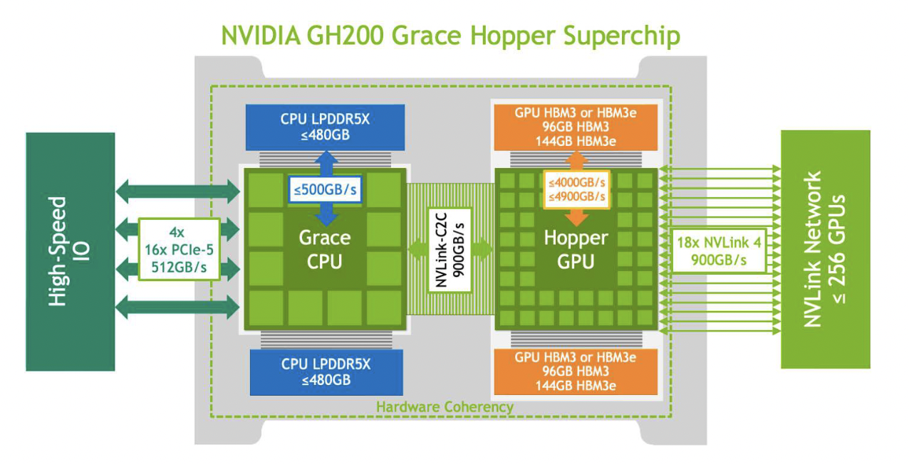
4. Grace Hopper GH100
In addition to the H100 models, NVIDIA has introduced the Grace Hopper Superchip (GH100). This is a total platform change from what we are used to seeing. I think this new concept of GPU processing by NVIDIA is being massively underplayed. It's both a good and a bad thing in my opinion.
At Nexgen Cloud, we have been doing R&D and benchmarking on this platform for a while now, and its performance numbers under some workloads are absolutely insane in comparison to ‘normal’ GPUs. In particular, any workload that has a good portion of CPU work required performs super well. This is explained by the ‘coherent' memory on these boards; the CPU and the GPU share the same memory, so any CPU-GPU communication latency basically goes out the window. Perhaps this can be compared to DMA and RDMA; it just removes a massive bottleneck in the system, and we see amazing performance as a result.
What I'm personally a little less excited about is this whole single vendor solution. NVIDIA is now manufacturing basically the entire server; they deliver a motherboard with RAM, CPU, and GPU all on a single board. This gives us great performance, but will we see a lack of innovation on these platforms as a result of a single vendor having total market dominance? There is still room for vendors to manage things like storage and connectivity, but I just worry that we won't see innovation in the sense we are used to in today's market that's driven by stiff competition and a need to build a USP to attract customers.
Side note: the GH100 seems to have slipped into the GH200.. So some of the specs and terminology seem to be getting mixed up between them, NVIDIA's messaging on this is awful :/
- Form Factor: Integrated CPU-GPU
- Memory: Up to 512 GB HBM3
- Memory Bandwidth: Up to 3 TB/sec
- TDP: Variable, depending on configuration
- Use Cases: Large-scale AI training and inference, data center acceleration, HPC simulations.
Pros:
- Integrated CPU-GPU architecture for improved performance.
- High memory capacity and bandwidth.
- Advanced interconnect technologies for enhanced scalability.
Cons:
- Complexity in deployment and configuration.
- Higher cost compared to standalone GPUs.
Addressing the Naming Confusion
The current naming convention of the H100 models can be confusing, especially given the variations in TDP, form factor, and use case. A more intuitive naming system, such as H101, H102, and H103, could help distinguish between the different models more clearly. I've pushed this more than once with the NVIDIA product team; I think they agree somewhat, but I'm not holding my breath, especially looking at the roadmap for Blackwell and Grace Blackwell. I think we are in for a world of pain in naming confusion… Perhaps it'll be my next topic for a LinkedIn post?
Here’s my suggestion:
H100 is the product line; it's the actual GPU itself, and the following are the actual deployment options:
- H101 for the PCIe variant
- H102 for the SXM5 variant
- H103 for the NVL variant
- GH101 for the current Grace Hopper variant
Critical Specs Comparison Table
| Model | Form Factor | Memory | Memory Bandwidth | NVLink Speed | PCIe Gen5 Speed | TDP | Use Cases |
|---|---|---|---|---|---|---|---|
| H100 SXM5 | SXM5 | 80 GB HBM3 | 3 TB/sec | 900 GB/sec | 128 GB/sec | 700W | HPC simulations, AI training, drug discovery, science |
| H100 PCIe | PCIe Gen 5 | 80 GB HBM2e | 2 TB/sec | 600 GB/sec | 128 GB/sec | 350W | Data analytics, medical imaging, fraud detection |
| H100 NVL | Dual PCIe | 188 GB HBM3 | Nearly 4 TB/sec | 600 GB/sec | 128 GB/sec | 400W(per card) | Advanced AI training, high-throughput inference |
| Grace Hopper GH100 | Integrated CPU-GPU | Up to 512 GB HBM3 | Up to 3 TB/sec | 600 GB/sec | 128 GB/sec | Variable | AI training, data center acceleration, HPC simulations |
Additional Notes and Sources
- The H100 models achieve gross margins exceeding 85% due to their advanced architecture and high demand:citation[oaicite:1]{index=1}.
- For the NVL models, NVIDIA H100 NVL cards use three NVIDIA NVLink bridges, providing 600 GB/s bidirectional bandwidth, significantly enhancing performance:citation[oaicite:0]{index=0}.
For more detailed specifications and performance metrics, you can refer to the official NVIDIA H100 documentation, NVIDIA GraceHopper Specs and performance analyses and AnandTech, my team at Nexgencloud doing their work on benchmarking each GPU.